MBE is low temperature process which is advantageous for VLSI technology. While preparing thin layers using MBE process, autodoping and autodiffusion both are minimized. The MBE process can be used for generating complicated doping profiles as it regulates the amount of dopant.
What is molecular beam epitaxy used for?
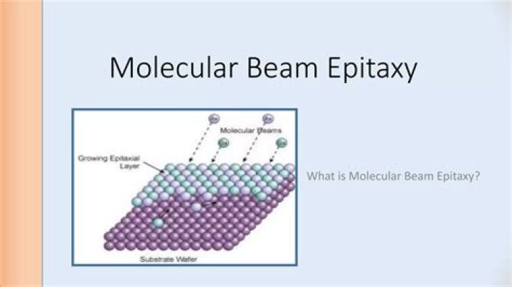
Molecular-beam epitaxy (MBE) is an epitaxy method for thin-film deposition of single crystals. MBE is widely used in the manufacture of semiconductor devices, including transistors, and it is considered one of the fundamental tools for the development of nanotechnologies.
What is molecular beam epitaxy method?
1.3. Molecular beam epitaxy (MBE) is a process in which a thin single crystal layer is deposited on a single crystal substrate using atomic or molecular beams generated in Knudsen cells contained in an ultra-high vacuum chamber.
What is an MBE system?
MBE System is a high performance tool which can be configured for a wide range of material applications. SVTA MBE systems offer an ultra-pure environment for precision fabrication of thin film structures for semiconductor, opto-electronic, photovoltaic, and magnetic applications.
What is the importance of vacuum in MBE?
4 SAG in MBE. MBE systems require an ultra-high vacuum environment, which reduces carbon contamination in the reaction chamber and can result in extremely high purity of the grown crystal.
Which epitaxy uses an evaporation method?
Molecular Beam Epitaxy
Molecular Beam Epitaxy is an evaporation process performed in an ultra-high vacuum for the deposition of compounds of extreme regularity of layer thickness and composition from well-controlled deposition rates.
Is MBE PVD?
MBE can be considered as a precise form of PVD. Solid source materials are placed in evaporation cells around a centrally placed, heated, substrate.
Why is molecular beam epitaxy MBE growth of crystals is done under ultrahigh vacuum UHV )?
Photo: Molecular beam epitaxy (MBE) in action. MBE takes place in ultra-high vacuum (UHV) chambers like this, at temperatures of around 500°C (932°F), to ensure a totally clean, dust-free environment; the slightest contamination could ruin the crystal.
What is meant by a molecular beam?
molecular beam, any stream or ray of molecules moving in the same general direction, usually in a vacuum—i.e., inside an evacuated chamber. In this context the word molecule includes atoms as a special case.
Why is epitaxy important?
The commercial importance of epitaxy comes mostly from its use in the growth of semiconductor materials for forming layers and quantum wells in electronic and photonic devices—for example, in computer, video display, and telecommunications applications.
What is epitaxy semiconductor?
Epitaxy is used in semiconductor fabrication to create a perfect crystalline foundation layer on which to build a semiconductor device, to deposit a crystalline film with engineered electrical properties, or to alter mechanical attributes of an underlayer in a way that improves its electrical conductivity.
